
 Sigma
Sigma
As a tech history fan, I've thought about writing on how image generation and storage have evolved in media. What we used to call cameras and video tape recorders. VTRs faded away about 20 years ago. Now, all storage is on platters or some type of RAM. Still, people often use the term video tape recording. So, I'm using it also.
What immediately follows is my understanding of the story. Feel free to jump to the end if you want. You can skip all the messy facts to where I try to use metaphors, analogies, and some allegories. It is there that the graphic above will hopefully make sense.
As I consider my approach, I realize there's an almost imperceptible 800‐pound gorilla. It's key to all the tech advances we've seen in the last 50 years. That of course is the microprocessor. Before we start to look at where this journey will take us, I will use a simple analogy and analysis to lay out the path I'll follow. It's mainly a numbers game. You throw as much pure mass as possible at anything you perceive to be a problem or goal to solve.
Before deciding how to measure processing power, I asked ChatGPT a question. I had a list of 17 microprocessors, two minicomputers, and one GPU, all from 1971 and onward.
The question: How soon would different processors need to begin to finish 10,000 calculations of π to 100 digits if they all must finish at the same time?
Parameters Used: Language: C and Assumptions: Unlimited memory/storage, dedicated computation. Before you mention that the earliest microprocessors had no high‐level languages and limited addressable memory, remember that these two factors helped level the playing field.
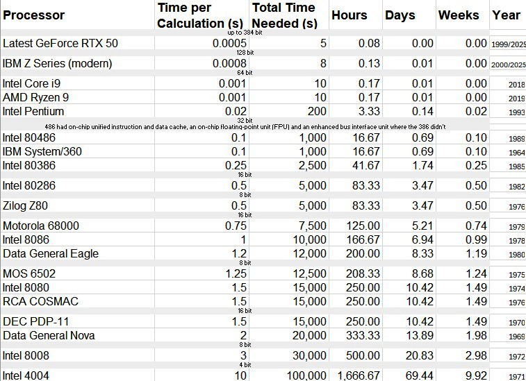
Some observations. You'll notice a note between the 486 and the Pentium. This, to me, was an inflection point. On the graphic at the top, you'll see where these devices went from the "moon" phase to the "planetary" phase.
Also, I find it interesting that the 8‐bit Z80 completed the tasks more quickly than the 16‐bit 68000.
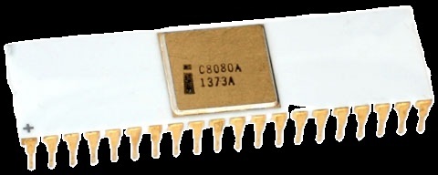
Intel 8080 came out in 1974. It is often called the first microprocessor with a higher‐level language compiler or interpreter, even if it was quite basic.
Early 8080s actually were a kit containing:
One 8080 microprocessor.
Four 1702A EPROM chips.
Eight 2102 SRAM chips.
Four 8212 non-programmable I/O port chips
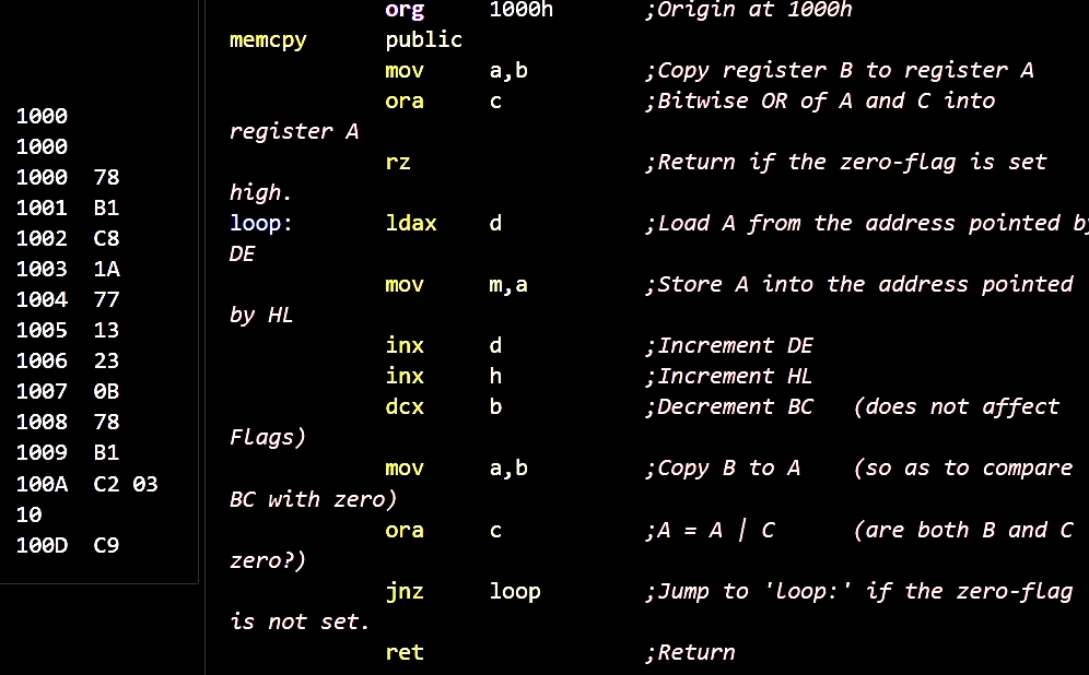
MOS Technology 6502 (1975) and Intel 8080 (1974) were the first microprocessors to have widely available interpreters and compilers for higher‐level languages.
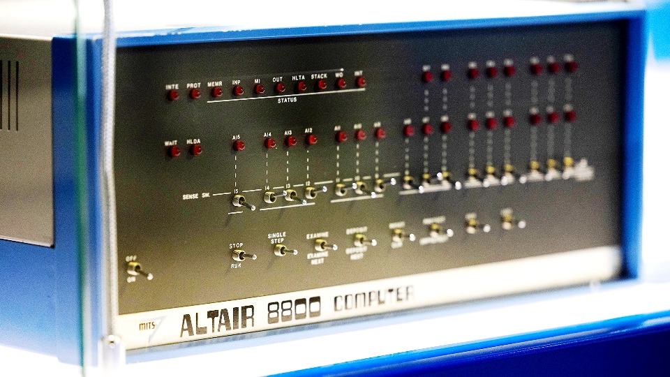
8080 was the one of the first micros to run BASIC (Beginner's All‐purpose Symbolic Instruction Code). Microsoft's first product was a version of BASIC for the Altair 8800 (which used the 8080).
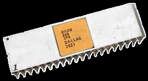
Zilog Z80 (1976) compatible with 8080 software but supported richer development environments. Commonly used in CP/M systems, an early OS that supported higher‐ level languages like FORTRAN, COBOL, and Pascal. The Z80 was also used in Radio Shacks TRS‐80.
The chart shows a massive difference in compute times. The first micro‐Intel 4004 was much slower than the fastest processor in 2025. In fact, the difference is 20,000 times. While not a shock comparing a 4‐bit processor to today's fastest GPU. But as we will see, there is a number that correlates to this increase in horsepower.
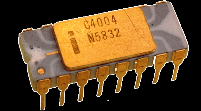
Starting with the Intel 4004 (1971): Transistor Count: ~2,300, Process: 10 µm, Word Size: 4‐bit
It was the first commercially available microprocessor. It was initially used in a calculator.
Next came the Intel 8008 (1972): Transistor Count: ~3,500, Process: 10 µm, Word Size: 8‐bit.
While the successor to 4004, it still had very limited capability.
Intel 8080 (1974): Transistor Count: ~6,000, Process: 6 µm, Word Size: 8‐bit
The 8080 was widely used in early personal computers.
MOS Technology 6502 (1975): Transistor Count: ~3,510, Process: 8 µm, Word Size: 8‐bit
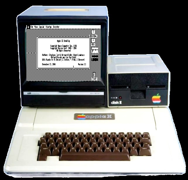
It was known for being very compact and cost‐effective compared to competitors. The 6502 stood out for its low transistor count. It was also designed efficiently, making it cheap and powerful for its time. The Apple I/II, Commodore 64, Atari 2600, and many other early systems used versions of it.
The 6500 took off in the way the 8080 never did. It wasn't better on paper ‐ but it was the right chip at the right price at the right time. While it had a smaller, more efficient instruction set. it had fewer registers, and it had half the clock speed of the 8080. It was dirt cheap. $25 in 1975, compared to $179 for the 8080. And it had another important design feature. Unlike other micros of the time, especially the 8080, it did not need multiple voltages to work. It only needed a single 5V supply.
The 6502 was designed by engineers who had left Motorola. They understood what embedded designers needed and stripped out everything unnecessary. It can be argued that this is the chip that first made personal computing accessible.
Intel 8088 (1979): Transistor Count: ~29,000, Process: 3 µm, Word Size: Internally 16‐bit, externally 8‐bit
The 8088 was a volume success, largely due to IBM. IBM famously chose the 8088 for the IBM PC (Model 5150) in 1981. This decision shaped the entire PC industry.
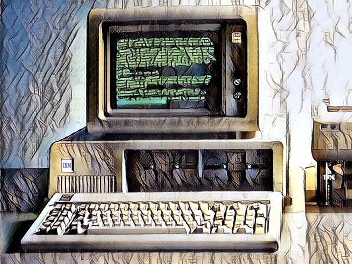
Why did IBM choose the 8088? It was cost‐effective, and could use existing, inexpensive 8‐bit support chips. The Intel 8086 was introduced earlier and had a 16‐bit data bus. It had scalable architecture. Like the 8086, it offered a full 16‐bit instruction set and could address 1MB of memory. IBM felt Intel was more established than upstarts like Zilog (Z80) or Motorola (68000).
The 8088 cost less to implement than the 8086. It had an 8‐bit external bus, which worked with older 8‐bit system designs.
The 8088 became the foundation of the x86 architecture. It kickstarted the "IBM PC compatible" ecosystem, which dominates computing to this day. The 8088 wasn't superior to the 8086. However, it was cheaper to produce. That's why the IBM PC and modern computing use this architecture today.
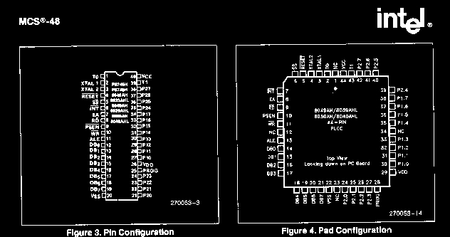
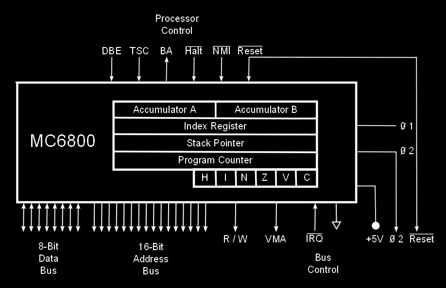
RCA and Zenith color TVs in the late 1970s) used Motorola 6800 or Intel 8048. They were used for channel memory, remote control, and on‐screen displays. The 8048 was considered a microcontroller and not a microprocessor. The 8048 and it's derivative the 8051 ended up in Microwave Ovens and other appliances.
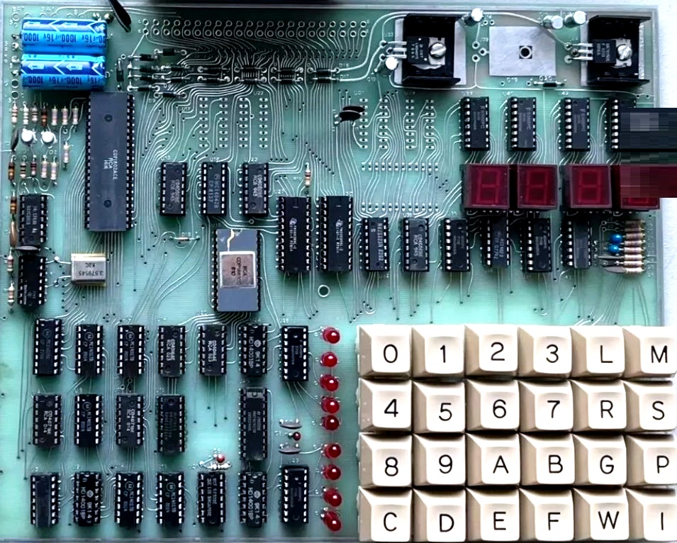
As you can see on the chart RCA introduced the Cosmac microprocessor in 1976. The COSMAC was meant for computers, but RCA entered the market slowly. Their efforts failed. This let other processors, like the MOS 6502, Intel 8080, and Zilog Z80, take charge. COSMAC found success in the embedded market. Its CMOS design let it operate at lower power, which was key to this achievement. By the late 1970s, it was common in several industries, particularly aerospace and automotive.
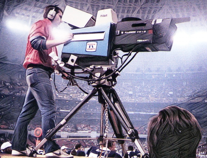
I ran across it as I went to school and worked on the RCA color camera, known as RCA TK‐47, which was introduced in 1979. It was RCA's flagship studio camera, notable for its fully automatic setup capabilities. The micro was used to setup and align the camera. This significantly reduced setup time and improved consistency across multiple camera units. I have a story that covers this aspect of the camera in the media section.
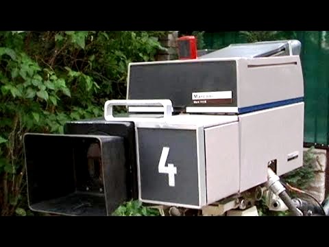
RCA wasn't the first, though. Marconi Mk VIII actually tried using a using an early microprocessor (circa 1971), possibly a 4004. It was an advanced color broadcast camera. It also offered full automatic setup. Challenges arose: The automatic alignment system sometimes adjusted during live broadcasts, causing operational issues, to put it mildly.
Let's take a moment and describe the difference between the two.
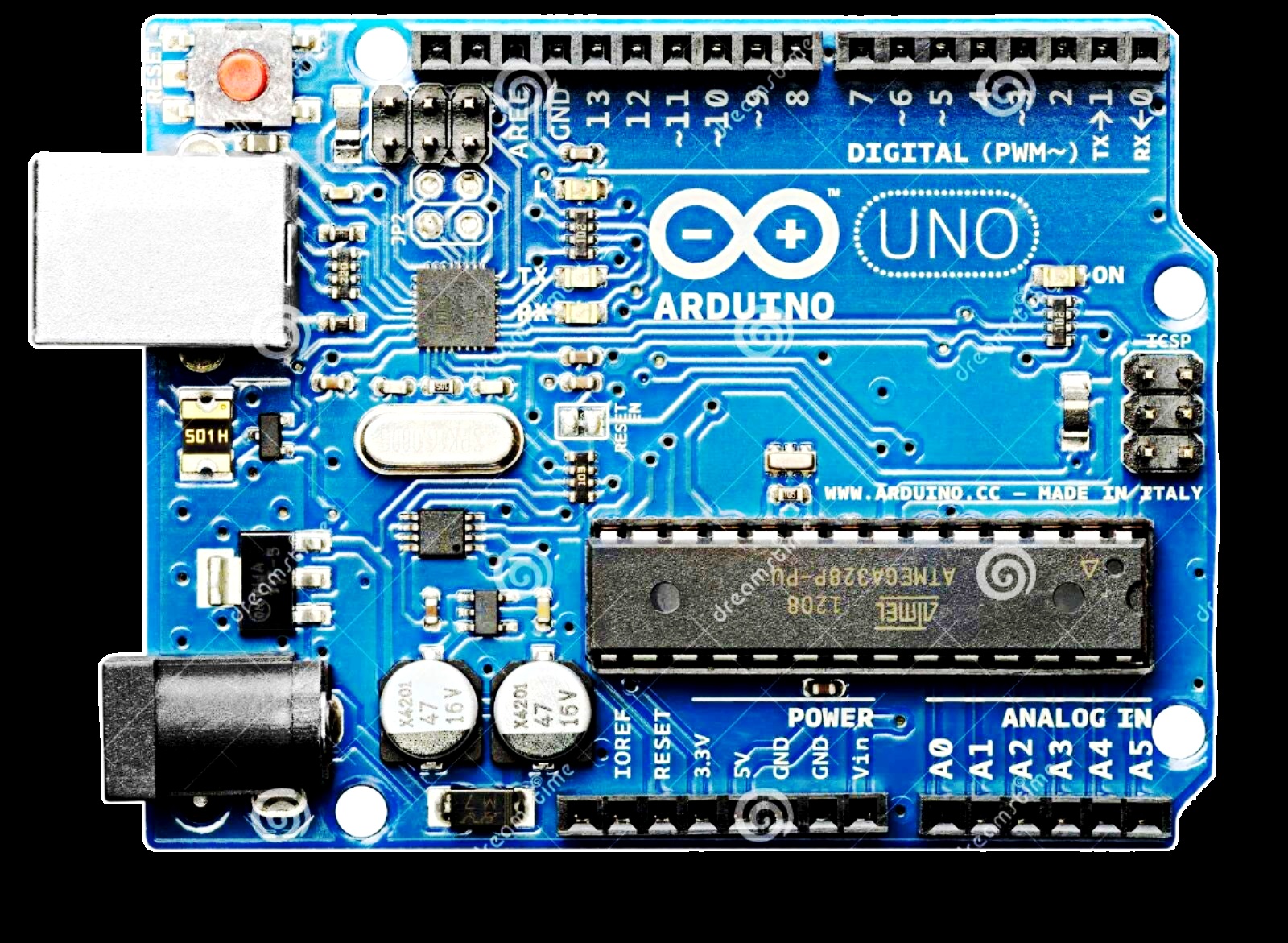
The difference between a microcontroller and a microprocessor lies mainly in what they include and how they are used. Microcontrollers (MCU). Generally, they were all‐in‐one chip: they contain a CPU, memory (RAM + flash), and input/output (I/O) peripherals on a single chip. They were used for specific tasks in embedded systems (like washing machines, thermostats, remote controls, etc.). They focused on control‐oriented applications. They were low power, low cost, and small size.
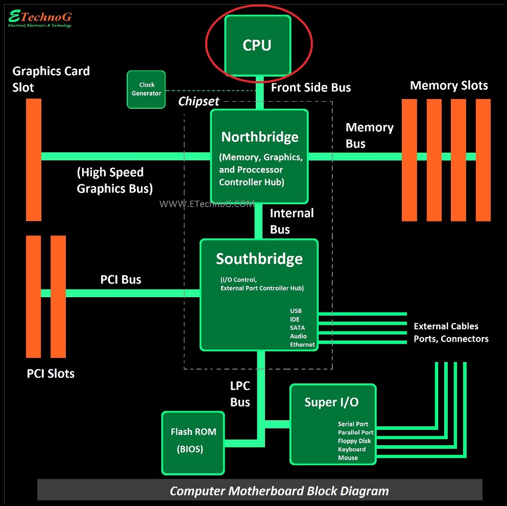
Whereas the Microprocessor (MPU) was a CPU only: it needs external memory, I/O, and support chips to function. They are used in general‐purpose computing, such as laptops, desktops, or servers. They are optimized for speed and versatility. Generally, they are more powerful, but more complex and expensive.
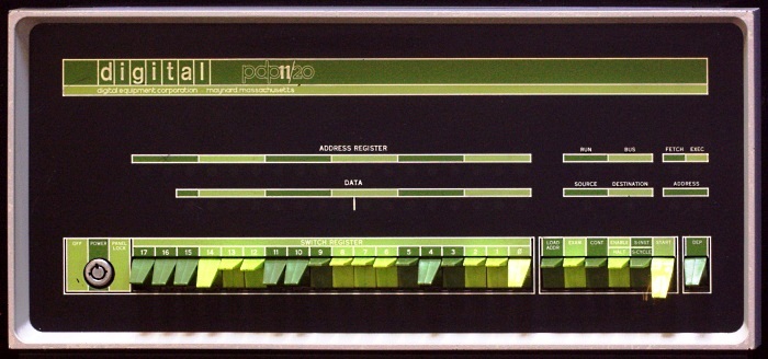
On the microprocessor performance chart, you may have seen three items that are complete computers, not just CPUs. These are the DEC PDP‐11 and Data General's Nova and Eagle "mini‐computers." Why are they included? By the late 70s, complete computers and PCs existed built around microcomputers. Yes, but well into the 80s and even into the '90s they still couldn't do what minis could do.
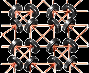
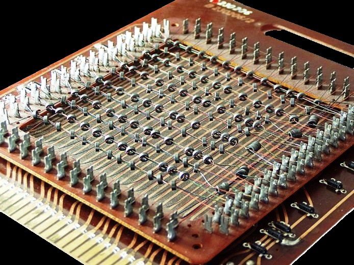
Its been claimed that the PDP‐11 inspired the architecture of the Intel x86 family, and the CP/M OS, which greatly influenced MS‐DOS.
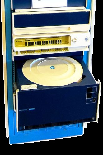
But first, I would like to make a comparison between microcontrollers and minicomputers. The microcontroller has features of both minicomputers and microprocessors. However, its design and use make it more similar to a minicomputer in real‐world applications. At least in how it provides standalone, self‐sufficient operation for specific tasks. A microcontroller acts like a minicomputer. It is hardware‐independent and self‐sufficient.
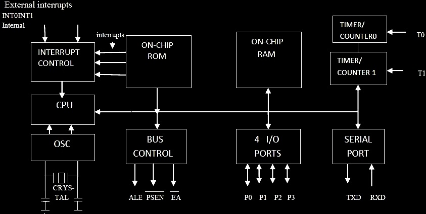
It's more like a basic microprocessor in terms of processing power and flexibility. Today, a microcontroller like an ARM Cortex‐M or an Arduino, can run a 3D printer or an IoT thermostat all by itself. This is similar to how a PDP‐11 controlled a CMC process in the past. Only the microcontroller is smaller and cheaper.
The author once worked for a company that made television editing equipment. Long before editing could be an app on you PC. Media (as it is called today) editing usually took up a small room in equipment. CMX, the company I worked for, used a PDP‐11. It was the heart of their control system. This system managed video tape recorders and other related equipment. The company made I‐squares (Intelligent Interface) along with editing software for the PDP‐11. The I‐square converted PDP‐11 commands to commands in a format that the equipment connected to a particular I‐square could understand.
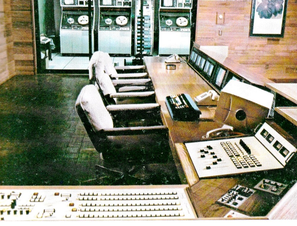
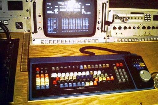
But why did these "minis" stick around? Early microprocessors like the Intel 4004, 8008, and 8080 were slow. They had a narrow bit width of 4 to 8 bits. Their addressing space was also very limited. Mini‐computers such as the PDP‐11 (16‐bit), VAX (32‐bit), and Data General Eagle (32‐bit) offered better performance. They had more memory capacity and could run complex operating systems and applications.
Minicomputers included: full operating systems, strong file systems, networking, and multi‐user support. They also supported disk storage, terminals, and industrial I/O. In contrast, early microprocessor systems were often basic or designed for one specific task.
Minicomputers had deep institutional investment in business, government, military, and university sectors. They powered manufacturing, lab equipment, data processing, and mission‐critical control systems. Minicomputers had mature development environments, debugging tools, and user support. Replacing them meant rewriting software, retraining users, and risking reliability.
Early micros often needed assembly language. They lacked high‐level language support, reliable compilers, and rich tool chains.
In the late 70s to early 80s, some companies blended the two. Microprocessors were embedded in mini‐computer peripherals or used as controllers. As was the case at CMX where the controllers (I‐squares) had an IPC‐16A PACE (Processing and Control Element). This was the first commercial single‐chip 16‐bit microprocessor, announced in late 1974.
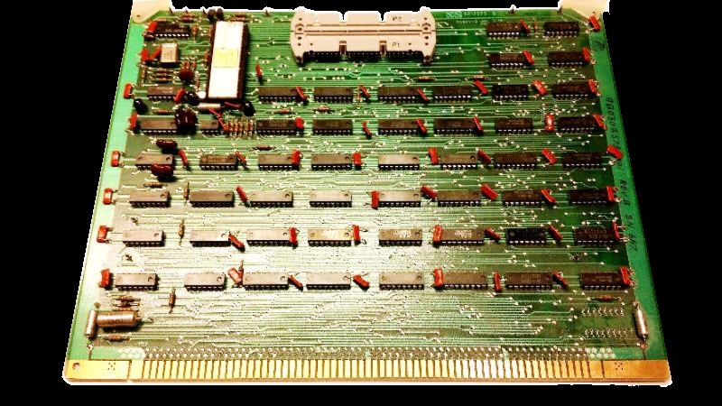
Microprocessors gradually grew powerful enough to take over. By the late 1980s to early 1990s, microprocessors (e.g., 386/486, Motorola 68000) caught up, thanks to: 16/32‐bit processing, larger memory addressing, UNIX and MS‐DOS support, and much lower cost. That's when minis gave way to workstations and PCs.
Motorola 68000 (1979): Transistor Count: 68,000, Process: ~3.5 to 5 microns, depending on the revision, Word Size: 16/32‐bit hybrid (internally 32‐bit, 16‐bit data bus)
Yes, the transistor count aligns with the name by design. The 68000 powered several devices. It was in the Apple Macintosh, Atari ST, and Commodore Amiga. It also ran the Sega Genesis and early Sun and HP workstations. The 68000 was a strong chip for its time. It had a large instruction set and addressing space. This made it popular in early desktop computers and embedded systems. Despite having far more transistors than previous micros, it remained reasonably affordable and accessible due to its clever design and Motorola's manufacturing capabilities.
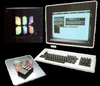
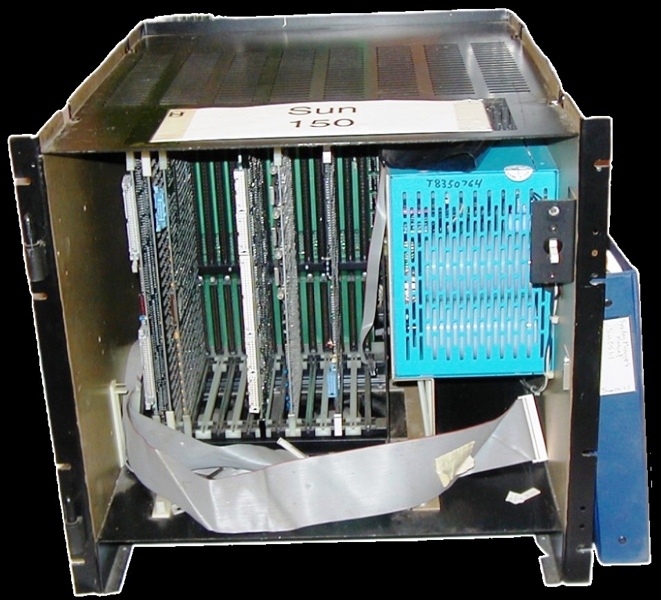
Intel 80286 (286) (1982): Transistor Count: ~134,000, Process Node: ~1.5 microns, Word Size: 16‐bit
It was used in the IBM PC/AT. This micro introduced protected mode, which enabled multitasking and instituted memory protection. It could address up to 16 MB of memory (vs. 1 MB in the 8086).
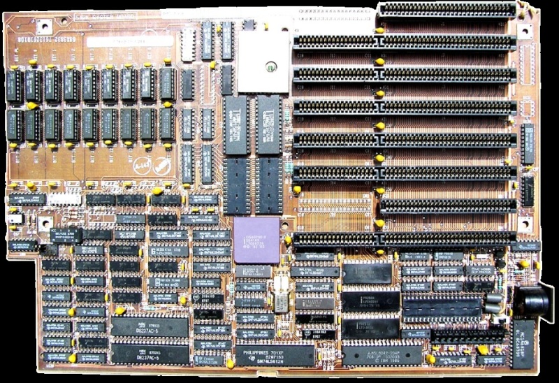
Intel 80386 (386) (1985): Transistor Count: ~275,000, Process: ~1.5 microns, Word Size: 32‐bit
This chip had both 32‐bit data and address buses, and virtual memory support. It also set the stage for modern PC operating systems like Windows and UNIX variants. The 386 established the 32‐bit computing foundation that lasted well into the 2000s.
Intel 80486 (i486) (1989): Transistor Count: ~1.2 million, Process: 1 µm, Word Size: 32‐bit
This micro has an Integrated FPU (Floating Point Unit). It featured 8 KB of on‐chip L1 cache and pipelined architecture for improved performance.
What stood out to me was the steady rise in transistor count. It started with 2,300 in the original 4004 and now, with the 486, exceeds a million. Now I realize that transistor count isn't everything, but it is a lot. After all, Motorola named a mainstay IC, the 68000, after its transistor count. It was introduced the same year as the 8088, which had less than half the semiconductors found in Motorola's offering.
In 1982, Intel jumped ahead of the 68000 with the 286. It more than doubled its transistor count. Over the next seven years, Intel launched the 386, and then the 486. The 486 had 9 times the transistor count that the 286 had.
What was allowing for these ever‐increasing transistor counts? The process for etching semiconductor die has consistently reduced the spacing between components. From 10µm in 1971 down to 1µm by 1985. Moore's Law shows that tech capability doesn't double every two years. Instead, it leaps forward every few years. Yet, it still averages out to what Moore said in 1965. We will look a little deeper at this later.
The shift from 486 to Pentium microprocessors began to push minicomputers off the stage. As workstations and PCs became more powerful, they could run UNIX or Linux and do what minis did for less money. Unix/Linux‐based minicomputers started being phased out in the late 1980s‐1990s.
Companies such as Sun Microsystems, HP, and DEC created "servers." These were basically modernized versions of minis.
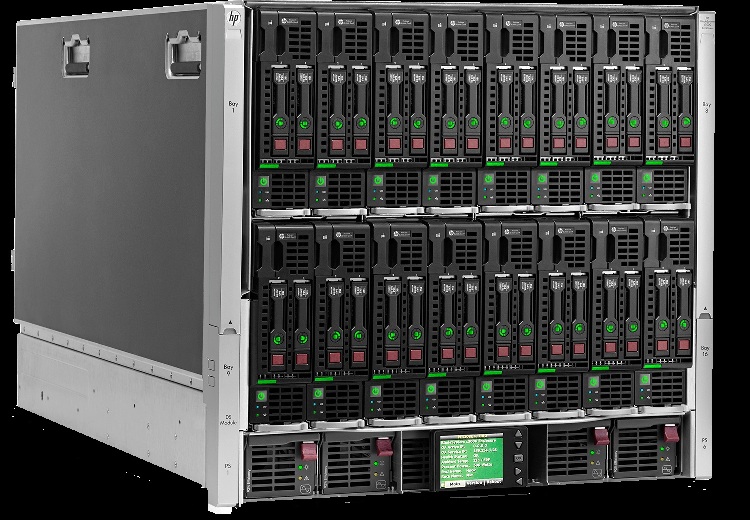
Intel Pentium and Xeon chips changed the game. Now, common hardware using Windows NT/2000 or Linux could manage traditional mini workloads, like files, databases, and control systems. These became "industry standard servers."
The idea of virtualizing multiple "minis" (now known as VMs or containers) on one physical machine was becoming standard.CPU virtualization allows one physical CPU to act like multiple virtual CPUs, known as vCPUs.
Intel Pentium (P5, original) (1993): Transistor Count: ~3.1 million, Process: 0.8 µm, Word Size: Superscalar 32‐bit
The micro had dual instruction pipelines, which were called superscalar. Superscalar refers to a processor's ability to execute more than one instruction per clock cycle by using multiple execution units. It also had a larger cache: 16 KB L1 cache (8K data, 8K instruction).
Plus, a faster FPU (floating‐point unit) math coprocessor than the 486. This chip, along with those that came after, marked a big leap in complexity and performance. The Pentium line started Intel's strong hold on desktop computing.
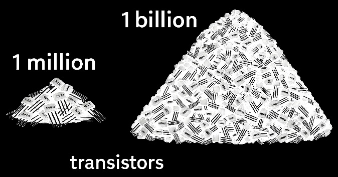
These chips marked a major leap in complexity and performance over their predecessors, with the Pentium line beginning Intel's modern dominance in desktop computing.
It didn't take long to get to the half‐way mark. The first general‐purpose microprocessor to reach half a billion (500 million) transistors was:
Intel Core 2 Quad (Kentsfield)(2006): Transistor Count: 582 million, Process: 65 nm
It was a dual‐die quad‐core processor (two dual‐core dies in a single package). This was not a monolithic 582 million transistors on a single die. It reached this total by combining two dies, each with about 291 million transistors. It was quad‐core design. It had 2 × 4MB L2 cache.
Intel's Yorkfield was the first monolithic quad‐core CPU. It had about 500 million transistors and was part of the Penryn family. It launched later with a 45 nm process. It was introduced in 2007. Penryn was a mobile processor from Intel. It came in different versions like Core 2 Solo, Core 2 Duo, Core 2 Quad, Pentium, and Celeron.
Notice the incredible decrease in die process technology. From the Pentium to the Penryn die the process has shrunk three orders of magnitude (x1000) times 17.77 (.8/.045). If we reduced the distance between New York City and Los Angeles by the same percentage, Los Angeles would be where Newark is, right across the Hudson!

Others were in the game, AMD being a notable one.
AMD's Phenom X4 (2007); Transistor Count: ~450M
While not quite at 500M, it is a notable competitor in that generation. This time marked the start of multicore dominance in desktop computing. More transistors were used for parallelism instead of just increasing clock speed.

Carl Sagan had a favorite word. That word x2 with a & in between was his trademark saying: "Billions & Billions." He mentioned the stars, but now it has a great observation about transistors in micros.
The first microprocessor to exceed 1 billion transistors was the:
Intel Itanium 2 (Tukwila) (2010): Transistor Count: 2 billion, Process: 65 nm
It has 4 cores, a massive 24 MB on‐die cache that is geared towards enterprise and high‐end servers. Tukwila was the first single‐die general‐purpose CPU to surpass a billion. Earlier, GPUs and multi‐chip processors had already crossed that milestone.
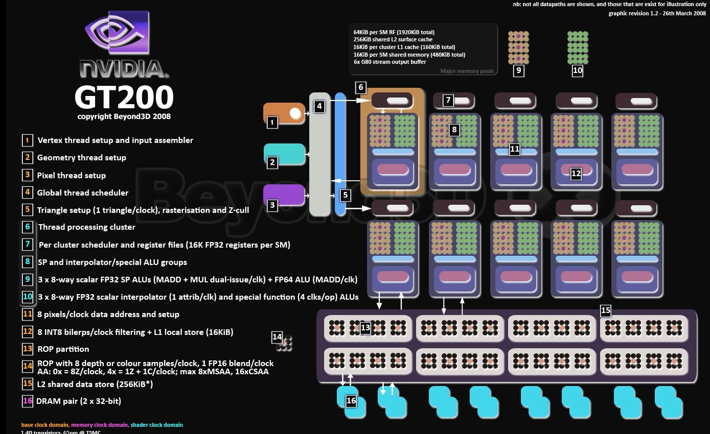
GPUs, such as the NVIDIA GT200 (2008), already had over 1.4 billion transistors. They are specialized parallel processors, unlike general‐purpose CPUs which are more serial in nature. Intel's Nehalem and Westmere families (2008–2010) got close but did not reach 1 billion per core or die.
So, Tukwila holds the title for microprocessors in the traditional CPU sense.
The NVIDIA GeForce RTX 5090 launched in 2025. It has an impressive 92.2 billion transistors. This high transistor count boosts performance in gaming and AI tasks. How was this massive compute engine possible? The process size is now down to 4nm.

The company behind this technology is Taiwan Semiconductor Manufacturing Company Limited. It's also called TSMC or Taiwan Semiconductor. It is a Taiwanese multinational semiconductor contract manufacturing and design company. It ranks among the world's most valuable semiconductor firms. It's the largest pure‐play semiconductor foundry and the biggest company in Taiwan. TSMC's custom 4N process node makes these advancements possible. It boosts transistor density and improves power efficiency.
Process node, or as I have been referring to it as simply process, is how close each node (transistor element) can be to each other.
Back to traditional CPUs. The transistor count in Intel Core i9 processors varies by generation, as Intel does not consistently disclose exact figures. However, estimates based on die size and manufacturing process provide approximate values:
Intel Core i9‐13900K (13th Gen, Raptor Lake): This chip uses the Intel 7 process node. It has about 100.76 million transistors per square millimeter. With a die size of 23.8mm x 10.8mm, the total transistor count is around 25.9 billion. (https://forums.tomshardware.com/)
Intel Core i9‐12900K (12th Gen, Alder Lake): The exact transistor count isn't published. However, it's likely a bit lower than the i9‐13900K due to being an earlier generation and using a similar manufacturing process. (https://forums.tomshardware.com/)
The transistor count in AMD Ryzen 9 processors varies by model and architecture. Here's a breakdown of some notable models:
Ryzen 9 5900X (Zen 3, 7nm), Configuration: 12 cores / 24 threads, Chiplets: 2 × CCDs + 1 × IOD, Transistor Count: Each CCD: ~4.15 billion transistors, IOD: ~2.09 billion transistors
Ryzen 9 5950X (Zen 3, 7nm), Configuration: 16 cores / 32 threads, Chiplets: 2 × Core Complex Dies (CCDs) + 1 × I/O Die (IOD), Transistor Count: o Each CCD: ~4.15 billion transistors. IOD: ~2.09 billion transistors, Total: ~10.39 billion transistors
Ryzen 9 7950X (Zen 4, 5nm). Configuration: 16 cores / 32 threads, Process: TSMC 5nm for CCDs, Transistor Count: ~13.1 billion transistors.
Let's briefly look at how these astronomical numbers of transistors shrunk to all fit on a single die.
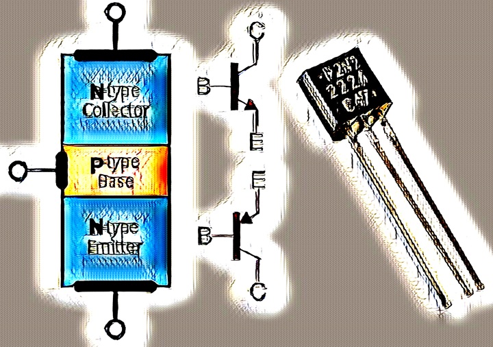
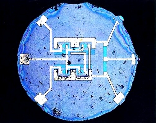
How was this incredible increase in density possible? In 1959, Fairchild Semiconductor invented the Planar Process. This method made it possible to create solid‐state devices, like individual transistors. Then, many transistors could be combined to form integrated circuits (ICs).
The main idea is to see a circuit as a two‐dimensional plane. We can use photography techniques, like film negatives, to block light. This prevents light‐activated chemicals from exposure.
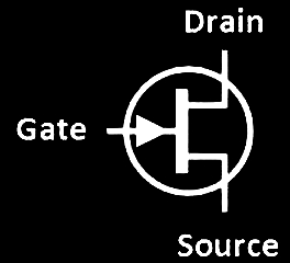
Early semiconductors typically used the metal‐oxide‐semiconductor field‐effect transistor (MOSFET). This type of FET is usually made by carefully oxidizing silicon. It has an insulated gate, the voltage of which determines the conductivity of the device. The MOS‐FET can change conductivity with voltage. This ability helps it amplify or switch electronic signals.
The main benefit of a MOSFET is that it uses very little input current. This helps control the load current in steady‐state or low‐frequency conditions. This is especially true when you compare it to bipolar junction transistors (BJTs). At high frequencies or during fast switching, a MOSFET needs a lot of current to charge and discharge its gate capacitance.
To make such a device, you start with a clean, flat surface. A silicon wafer, completely smooth, like a blank canvas. Your design is converted to a mask. A light‐sensitive chemical layer is spread over the silicon wafer. Light is shined through a mask, similar to a stencil. This forms patterns that match the circuitry. Chemicals are added to remove exposed parts. They carve tiny channels and shapes.
Materials, like metals or dopants, are added to the patterns. This makes them either conduct electricity or not. This creates the tiny switches (transistors) that control how electricity flows. Repeat for additional layers. This is done again and again, stacking up layers and connecting them, like building multiple floors of that tiny building.
How did chipmakers change from big circuits (10 micrometers) to tiny circuits (7 nanometers)?
The goal shifted to packing more transistors into the same area. This meant creating thinner lines. It was like going from a marker to a fine pen, and finally, to a laser pointer.
To make that happen, the chipmakers needed better tools and materials.
What Made It Possible?
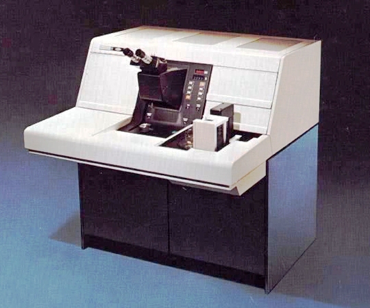
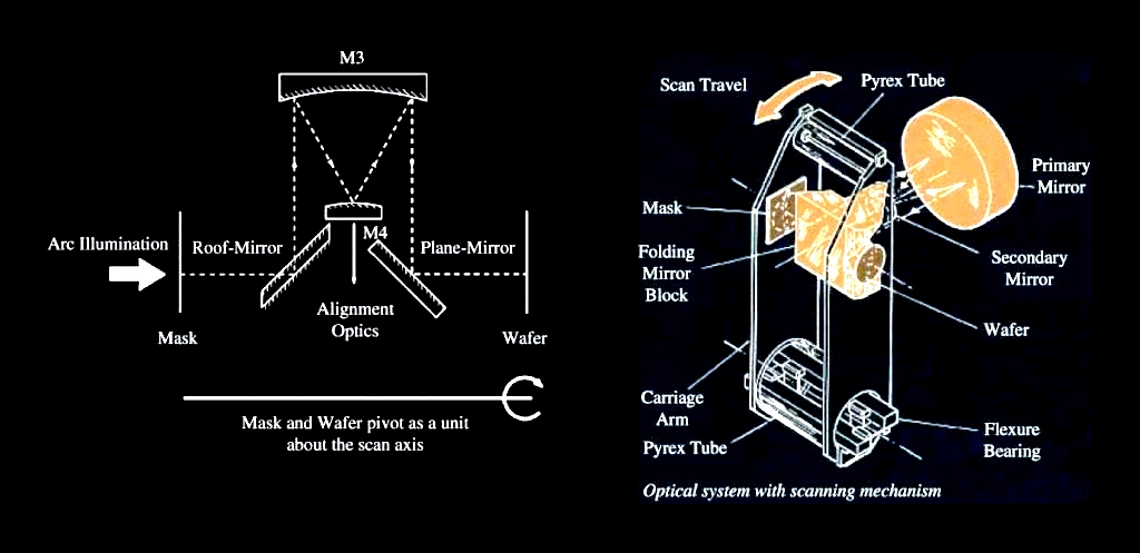
Early machines used visible or UV light. This limited how small you could print. Next, deep UV offered better resolution. Immersion followed, which involves placing water between the lens and chip to reduce the image size.
Then came EUV, or Extreme UV light, which is like using a magnifying glass with sunlight to create fire. It allows chipmakers to draw very small lines.
New Transistor Shapes (3D Transistors) were introduced. Flat transistors stopped working well when they got too small. So, engineers started stacking them upright. This is like building skyscrapers instead of houses. This saved space and power.
The use of smarter materials. They used improved insulators and metals to prevent electricity from leaking through small gaps.
Atomic‐Level Coating and Polishing. When the parts become smaller than bacteria, surface bumps and gaps become a big problem. So they invented tools that could coat, smooth, and build surfaces one atom at a time.
The use of Supercomputer Software. At these tiny sizes, engineers can't draw the chip layouts by hand anymore. So special software now designs circuits and checks for flaws before the chip is even built.
Let's start to wrap up by briefly discussing how today's advanced microprocessors use billions of transistors effectively.
Today's top microprocessors, like the Intel Core i9, AMD Ryzen 9, and NVIDIA's newest GPUs, pack a lot of power. To unlock their full potential, you need smart software. You also need efficient system design and programming strategies that fit how these chips work.
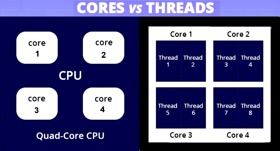
First off Parallelism is Key. Modern processors have many cores and threads. Often numbering 16‐64 cores, and two or more threads per core, and GPUs can have thousands of smaller cores.
A core can support multiple threads. However, how many can run at once depends on a few factors. This includes the cache size of the core, its speed, and the types of instructions processed. A core can run multiple threads at once, but there's a limit to how many can run at the same time. Hyper‐Threading splits each physical core into two or more logical processors.
To effectively use all the cores you need optimized software. You need multi‐threaded code in the OS, which uses multiple CPU cores at once. This means parallel rendering, simulations, and server functions. This must be task‐based programming which breaks large tasks into smaller ones and runs them concurrently.
That OS must incorporate GPU acceleration. If it sees parallel‐heavy tasks, such as AI, video rendering, etc) it offloads it to GPUs using application acceleration software. Common libraries include CUDA, OpenCL, or DirectML.
Instruction‐Level Optimization with advanced CPUs support. Like using Single Instruction and Multiple Data (SIMD) which lets one CPU instruction do the same task on many data points at once. This enhances processing speed and efficiency. Also, out‐of‐order execution. Here the hardware reorders instructions for faster execution. It reminds me of MPEG. In MPEG, video frames aren't sent in chronological order. Instead, they are sent in the order that makes decoding faster.
Other Compiler & software tricks such as using compilers that support vectorization. Vectorization is when the compiler spots simple, repetitive work (like adding numbers in a list). It then groups these together. The tells the CPU to do many operations at once, instead of one at a time. This uses special hardware in the CPU called SIMD units which we mentioned above.
Another trick is to use assembly code for very important routines that need to run quickly.
A third area is memory and cache optimization. Modern CPUs have layered caches (L1, L2, L3), and performance hinges on keeping data close to the core.
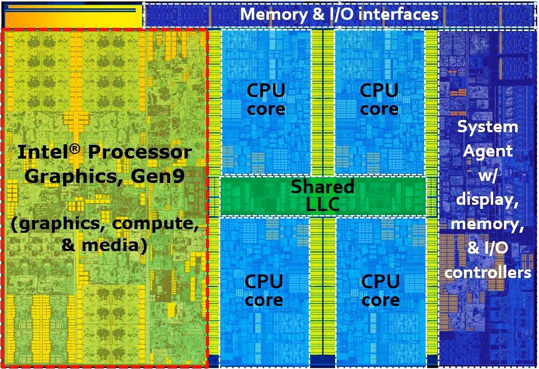
A fourth area is Hyperthreading / SMT (Simultaneous Multithreading). As already mentioned most modern CPUs can run at least two threads per core. To optimize this the software needs proper thread scheduling, not overload or underutilize threads.
Balance workloads across cores and NUMA zones in servers. Non‐Uniform Memory Access (NUMA)(NUMA) applies to multi‐CPU or multi‐core systems (like dual‐socket servers). It means each CPU or group of cores has faster access to some RAM local memory physically. Accessing RAM connected to another CPU (remote memory) is slower. So access time depends on where the memory is in relation to the core asking for it. That's why it's called "non‐uniform."
Use workload‐specific optimization. Different workloads benefit from different architectures.
Use tensor cores for AI/ML (Machine Learning). These are special processing units in NVIDIA GPUs. They speed up matrix operations, which are key for deep learning tasks. With Apple and Intel, use Neural Processing Units. These are also called AI accelerators or deep learning processors. They are a type of specialized hardware accelerator.
For video production, offload encoding/decoding to specialized media engines. For scientific computing, use high memory bandwidth and double‐precision support.
The OS and its scheduler should have CPU topology awareness as to the type of cores available. A lot of the various execution approaches above are based on the type of core it is. Developers work to get the right mix of cores. The OS should assign a task to the most efficient core available.
First there are General‐Purpose Cores. They are standard cores designed for a wide range of tasks. They are found in desktops, laptops, and servers. Examples include the Intel Core, AMD Ryzen, Apple M‐series performance cores. Intel "P‐cores" (Performance cores in Alder Lake and beyond), ARM Cortex‐A series (high‐performance mobile cores), Apple's "Firestorm" or "Avalanche" in M‐series chips.
Next High‐Performance Cores (a.k.a. "Big Cores"). They are powerful cores optimized for speed and complex tasks. They are used for gaming, video editing, 3D rendering, etc. Examples include the Intel "P‐cores" (Performance cores in Alder Lake and beyond), ARM Cortex‐A series (high‐performance mobile cores) and Apple's "Firestorm" or "Avalanche" in M‐series chips.
Next are Power‐Efficient Cores (a.k.a. "Small Cores"). They are simpler, low‐power cores designed to save energy. They are used for background tasks, mobile standby, and battery conservation. Examples include Intel "E‐cores" (Efficient cores), ARM Cortex‐A55, Apple's "Icestorm" or "Blizzard" cores.
We talked about this earlier. Not a different core type, but a feature of many general‐purpose cores. Turns out it takes Hyper‐Threaded/Simultaneous Multi‐Threading (SMT) enabled cores to accomplish. These are cores that can handle two threads at once (acts like two virtual cores).
Out‐of‐Order vs. In‐Order Cores. Turns out not all cores can use this trick either. You need Out‐of‐Order Execution Cores which reorder instructions for efficiency. these are faster, more complex, and consume more power than regular cores.
There are Server‐Specific Cores. They optimized for concurrency, data throughput, and long uptime. Examples: AMD EPYC cores, Intel Xeon cores, IBM POWER or Z‐series cores.
And of course, you must have Specialized or Accelerated Cores. They are cores designed for specific functions, often seen in System on a Chip (SoCs). Examples: Signal Processing Cores used in image/video/audio processing, Neural Processing Units (NPUs) ‐ AI workloads, Security Cores ‐ handle encryption or secure boot tasks GPU Cores, not CPU cores but used alongside them for parallel tasks. They are used in Smartphones & tablets (e.g., Apple A17, Qualcomm Snapdragon), Smart TVs, game consoles, Embedded systems/IoT devices, some desktops and mini‐PCs.
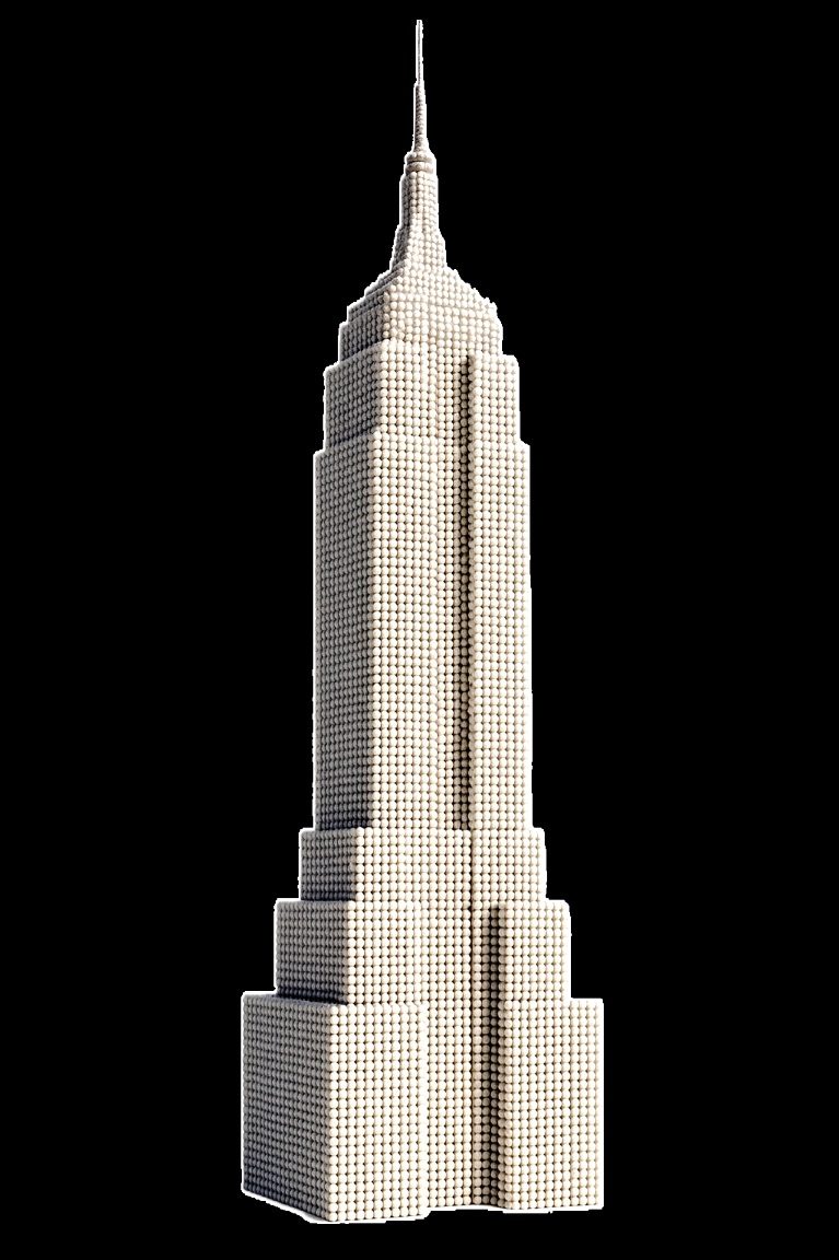
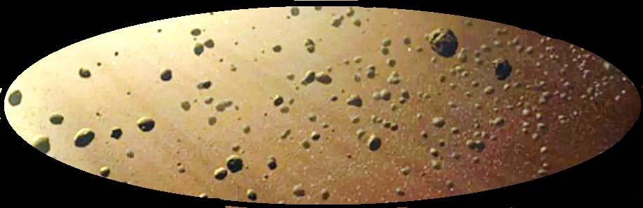
At first, in the dusty world of computing, the first microprocessors were tiny. They were like small asteroids floating in a vast digital space. The MOS Technology 6502 was one of the earliest. It stood out like a small stone in a vast starfield of possibilities. It was simple and compact. It powered early home computers, video game consoles, and embedded systems. Yet, it had the potential for something much bigger.
As technology advanced, computing power grew. A new generation emerged. Small by astronomical standards, but still expanding. The Intel 8088 and 8086 are close cousins. They set the blueprint for future Intel chips. Small asteroids and other debris began to clump together. They started to appear, like small moons gently shining in the dark sky of computing. These chips had more complexity and functionality. They still stayed near the limits of what was possible.

Then came a revolution: the Intel 486. This processor was so advanced for its time that if computing power were mass, it would rival the Moon. It made a statement in the night sky. The 486 had floating‐point capability and better instruction throughput. It was a platform for building new possibilities. Software began to evolve alongside it, making full use of the terrain it provided.

Not long after, the Pentium processor ignited the next age. This I will call the age of planets. It was no longer just space debris. The Pentium was a small world. It barely made it to the big league, as its representative was Mercury in size. Now, software thrived with color, motion, and sound.
As microprocessors evolved, they climbed the planetary scale. The Intel Core i9 is one of the most powerful CPUs today. It's as strong as Jupiter is big in the world of computing. Fast, multi‐core, and hyper‐threaded, it offers huge computing power. It can run big apps, multitask well, and handle advanced AI and machine learning tasks.

Now, even bigger beasts surround it. These are GPU‐based processors, like NVIDIA's RTX series. They are like cosmic titans or even stars. They can blaze with what soon will be trillions of transistors, changing what computing means. GPUs are starting to condense in larger clumps of mass. At some point, the gravity from all that mass will start "fusion." One might wonder when humankind will no longer be a part of the computing revolution.

This journey from asteroids to Jupiter highlights how transistors and processing speed have improved. It also marks a revolution in what humans can do. We started by writing BASIC programs in garages. Now, we simulate the universe on GPUs. We've built a solar system of silicon, and with or without us, that universe will go on creating more.
